
Decoding the technologies of tomorrow, today.
Exploring the breakthrough innovations shaping our world. From AI infrastructure and robotics to biotech, quantum computing, and spatial tech.
Exploring the breakthrough innovations shaping our world. From AI infrastructure and robotics to biotech, quantum computing, and spatial tech.
For much of the modern computing era, semiconductor manufacturing depended on a remarkably specialized international supply chain. Chip designs could originate in the United States or elsewhere, wafers could be processed at highly specialized foundries in East Asia, advanced components could be packaged and tested in different countries, and finished devices could then move through a global electronics network.
That model delivered extraordinary efficiency, but it also created dependencies that were easy to overlook when chip demand was relatively predictable.
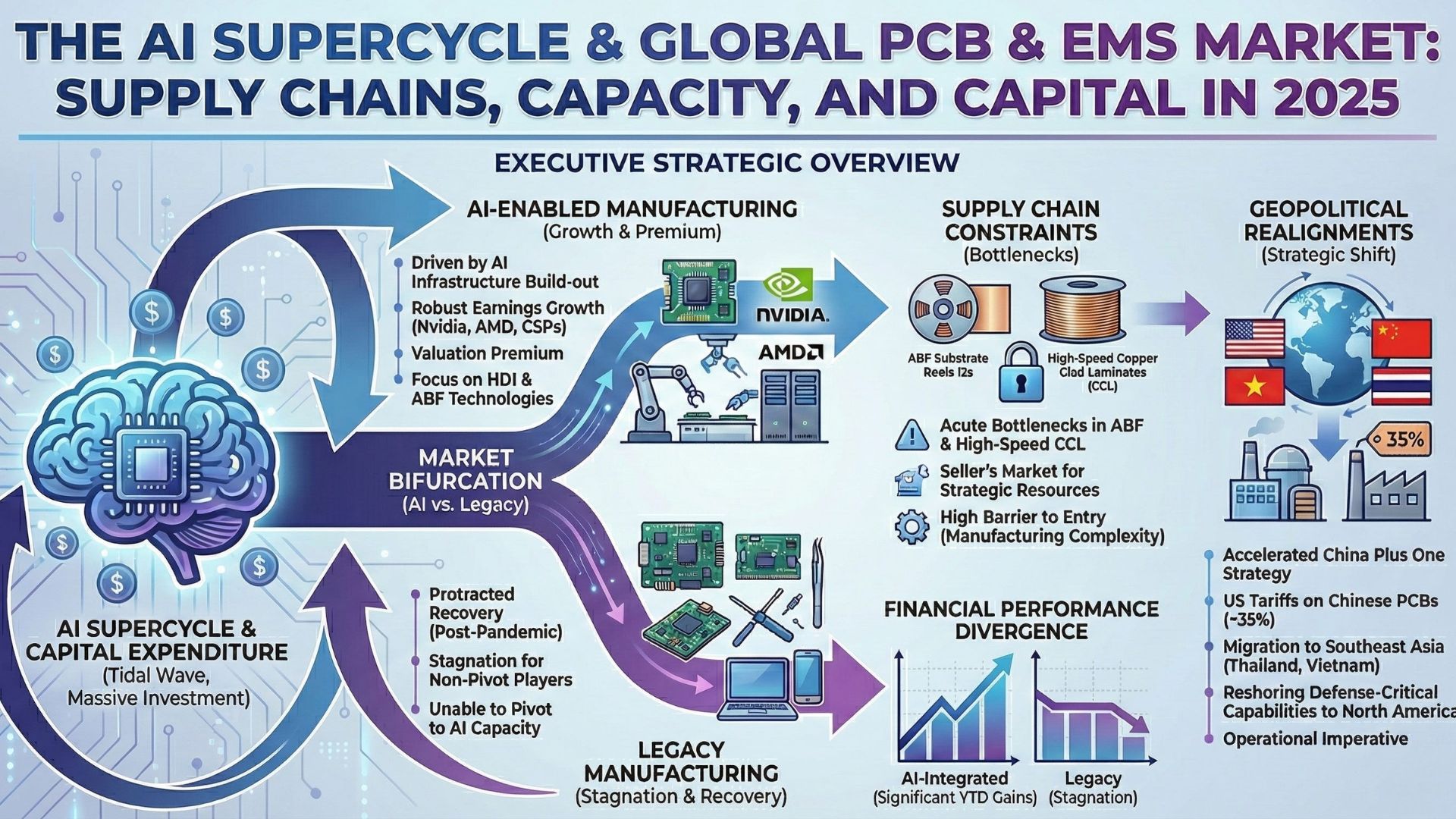
The rapid expansion of generative AI has changed the equation. Advanced accelerators require leading-edge logic, high-bandwidth memory, sophisticated packaging, and large volumes of specialized manufacturing capacity. Demand is rising across several of those layers at once, making bottlenecks more visible and exposing how difficult it can be to expand semiconductor production quickly.
Building an advanced AI processor is therefore much more complicated than sending a design file to a fab. The process depends on specialized materials, precision manufacturing equipment, advanced packaging, highly trained workers, and enormous capital commitments. The result is a supply chain in which a constraint at one stage can affect production much further downstream.
One of the defining characteristics of advanced semiconductor manufacturing is how concentrated it remains.
Many leading AI accelerators are built using advanced logic process nodes, including 5nm- and 3nm-class technologies, with newer designs moving toward 2nm-class manufacturing. These node names describe generations of semiconductor process technology rather than literal transistor dimensions, but they indicate how far the industry has pushed fabrication complexity.
Only a limited number of foundries currently have the process technology, manufacturing capacity, and yields required to produce leading-edge logic at commercial scale.
That concentration creates several risks.
A large share of leading-edge semiconductor manufacturing capacity is concentrated in East Asia, particularly Taiwan and South Korea. These manufacturing hubs also face natural hazards, including earthquakes and water-supply constraints, as well as broader geopolitical risks.
A disruption does not have to destroy a factory to create a problem. Temporary restrictions on electricity, water, transportation, equipment servicing, or component deliveries can affect production schedules.
Semiconductor fabs cannot be expanded like conventional warehouses.
A leading-edge facility requires years of construction, equipment installation, qualification, and process ramp-up. The full path from an investment decision to meaningful production can therefore extend well beyond the construction period itself.
That creates an uncomfortable mismatch with AI demand. Accelerator orders can increase rapidly, while new semiconductor capacity arrives on a much slower timetable.

For years, discussions about semiconductor manufacturing tended to focus on front-end fabrication: lithography, transistor formation, wafer processing, and yield.
AI accelerators have made another part of the process much more important.
Modern high-performance processors increasingly combine compute dies, memory interfaces, input/output components, and high-bandwidth memory in sophisticated packages. Instead of putting every function onto one enormous monolithic piece of silicon, designers can divide functions across multiple dies and connect them using advanced packaging technologies.
Chiplets, 2.5D integration, and 3D stacking are examples of approaches used to increase integration while managing the practical limits of very large monolithic chips.
Traditional wire-bonding remains useful across many semiconductor products, but it is not sufficient for many of the most demanding AI accelerator packages, where extremely dense and short interconnects are required.
That creates another capacity constraint.
Foundries, OSAT providers, memory manufacturers, and other packaging specialists all have to coordinate processes that demand tight alignment between dies, substrates, interconnects, and thermal solutions. Defects in a critical interconnect or die can reduce package yield and, in some cases, render an expensive multi-die assembly unusable.
The result is straightforward: adding more wafer capacity does not automatically solve an accelerator shortage if advanced packaging remains constrained.
The semiconductor supply chain extends far beyond fabs and packaging facilities. It depends on a large ecosystem of specialized machinery, chemicals, gases, wafers, substrates, and precision components.
Some of those dependencies are particularly difficult to replace.
Extreme ultraviolet lithography is one of the clearest examples.
ASML is currently the sole commercial supplier of EUV lithography systems used for leading-edge semiconductor manufacturing. These machines are extraordinarily complex and depend on an enormous network of specialized components and suppliers.
That makes EUV equipment a strategic bottleneck.
A fab cannot simply order an equivalent machine from another supplier if delivery is delayed. The manufacturing ecosystem surrounding EUV equipment therefore has consequences far beyond the equipment itself.
Advanced fabs also consume large quantities of highly purified gases and chemicals.
Their requirements are stringent because even small amounts of contamination can affect manufacturing yields. Semiconductor companies therefore rely on specialized purification, storage, transportation, and recycling systems.
Neon supply illustrates another dimension of the problem. Ukraine was historically an important source of purified neon used in semiconductor-related laser systems, and the disruptions associated with the war highlighted the risks created by regional concentration. The industry has since worked to diversify supplies and expand recycling capacity.
The broader lesson is important: a material can represent a small fraction of a chip's total cost while still being essential to the manufacturing process.
Silicon itself is abundant, but semiconductor-grade wafer production requires extremely high levels of purity, dimensional control, and surface quality.
The same principle applies to other components of the manufacturing chain. Specialty chemicals, photomasks, substrates, gases, and equipment parts may each come from relatively small groups of qualified suppliers.
Replacing one supplier is not necessarily as simple as switching vendors. A new material or component may require extensive testing and process qualification before it can be used in high-volume manufacturing.

These dependencies have encouraged governments and semiconductor companies to rethink how much manufacturing capacity should be concentrated in a small number of regions.
In the United States, the CHIPS and Science Act has supported efforts to expand domestic semiconductor manufacturing and research. Japan and European countries have pursued their own programs aimed at strengthening semiconductor capacity and reducing selected supply-chain dependencies.
The objective is not necessarily complete self-sufficiency.
That would be extremely difficult because modern semiconductor production is inherently international. A single advanced processor may involve design work, wafer fabrication, memory production, packaging, equipment from multiple countries, and materials from many more.
The more realistic goal is resilience: creating enough geographically distributed capacity that a disruption in one region does not immediately become a global production crisis.
A new fabrication plant is only one part of the equation.
Advanced semiconductor facilities require engineers, equipment technicians, process specialists, materials scientists, and other highly trained workers.
As countries build new fabs, they also have to develop the workforce capable of operating them. That can take years because many of the required skills are highly specialized and are learned through direct experience with manufacturing equipment and processes.
A fab also needs an ecosystem around it.
Chemical suppliers, equipment maintenance companies, waste-treatment providers, logistics firms, testing services, cleanroom contractors, and other specialized businesses all contribute to stable operations.
This is one reason semiconductor manufacturing tends to cluster geographically. Once a dense supplier network exists, companies benefit from shorter logistics chains, specialized labor pools, and established technical relationships.
Recreating that environment in a new region is considerably harder than constructing the factory itself.
The AI hardware boom is therefore not simply increasing the number of chips the world needs. It is changing which parts of the semiconductor ecosystem matter most.
Leading-edge logic remains critical, but so do high-bandwidth memory, advanced packaging, substrates, lithography equipment, specialty chemicals, and the manufacturing capacity needed to bring all of those components together.
That creates a more complicated definition of supply-chain resilience.
A region may have substantial wafer capacity but limited advanced packaging. Another may have strong packaging capabilities but depend heavily on imported equipment. A third may produce important chemicals but lack sufficient local semiconductor manufacturing.
Resilience is consequently a network problem rather than a single-factory problem.
The semiconductor industry is likely to remain globally interconnected even as governments push for greater regional capacity.
The economics make complete decoupling difficult. Advanced fabs cost enormous amounts to build, semiconductor equipment is highly specialized, and many manufacturing processes depend on suppliers that have spent decades developing narrow areas of expertise.
At the same time, the cost of excessive concentration has become more visible.
For AI companies, a shortage of accelerators is not necessarily caused by a shortage of silicon wafers. It could originate in advanced packaging, high-bandwidth memory, substrates, equipment availability, or another part of the manufacturing chain.
That distinction matters because expanding the wrong part of the supply chain will not remove the actual bottleneck.
The rapid growth of AI computing has exposed how dependent modern technology is on a deeply interconnected semiconductor manufacturing system.
Leading-edge fabs remain essential, but they are only one piece of the puzzle. Advanced packaging, high-bandwidth memory, lithography equipment, specialty materials, skilled workers, and regional supplier networks all determine how quickly the industry can turn chip designs into working AI hardware.
The response is unlikely to be a simple shift from global manufacturing to completely local production. A more practical approach is to build additional capacity across key regions, diversify critical inputs, expand advanced packaging capabilities, and maintain enough redundancy to absorb disruptions.
AI progress ultimately depends on more than better algorithms or faster accelerator architectures. It also depends on whether the physical supply chain can manufacture those systems at the scale the computing industry demands.