
Decoding the technologies of tomorrow, today.
Exploring the breakthrough innovations shaping our world. From AI infrastructure and robotics to biotech, quantum computing, and spatial tech.
Exploring the breakthrough innovations shaping our world. From AI infrastructure and robotics to biotech, quantum computing, and spatial tech.
Cloud AI gets most of the attention because its infrastructure is hard to miss: huge server clusters, specialized accelerators, and data centers built around enormous computing loads. At the same time, more AI inference is moving in the opposite direction, toward smartphones, cameras, wearables, industrial controllers, and other devices where data is generated.
This is the world of edge AI. Instead of sending every inference request to a remote server, the device performs at least part of the machine-learning workload locally. That can reduce response latency, keep selected workloads running without a constant cloud connection, and limit the amount of sensitive data that has to leave the device.
The hardware challenge is very different from building an AI server.
A data center can provide substantial electrical power and use large cooling systems to remove heat. A phone, camera, or industrial sensor has far less room to work with. Designers have to fit useful AI performance into a tightly controlled thermal and power envelope, often while keeping the device small, quiet, inexpensive, and reliable.
That makes edge AI hardware a balancing act between compute performance, memory access, power consumption, and sustained temperature.
Physics becomes difficult to ignore when AI processing moves into compact hardware.
A data center accelerator can be paired with sophisticated airflow systems or liquid cooling loops. A wearable device may have little more than its enclosure and a small amount of passive heat spreading. An industrial sensor might be sealed against dust and moisture, leaving very limited options for active cooling.
The allowable temperature also depends on the device. Semiconductor manufacturers specify operating and junction-temperature limits for particular chips and packages, and those limits vary across consumer, industrial, automotive, and other applications.
Power budgets can be just as restrictive.
A battery-powered wearable may need to keep average consumption within a relatively small range so that the battery lasts through normal use. A smart camera connected to a wall adapter has more room, while an industrial device powered through Power over Ethernet operates within the limits of its particular network and power architecture.
The important distinction is between peak performance and sustained performance.
A processor that reaches a very high frequency for a short burst may look impressive in a benchmark, but that figure tells little about what happens when the workload continues for several minutes. If temperature rises enough to trigger frequency or voltage reductions, sustained throughput can fall well below the initial peak.
For edge AI, thermal design therefore has to be considered alongside the compute architecture from the beginning.

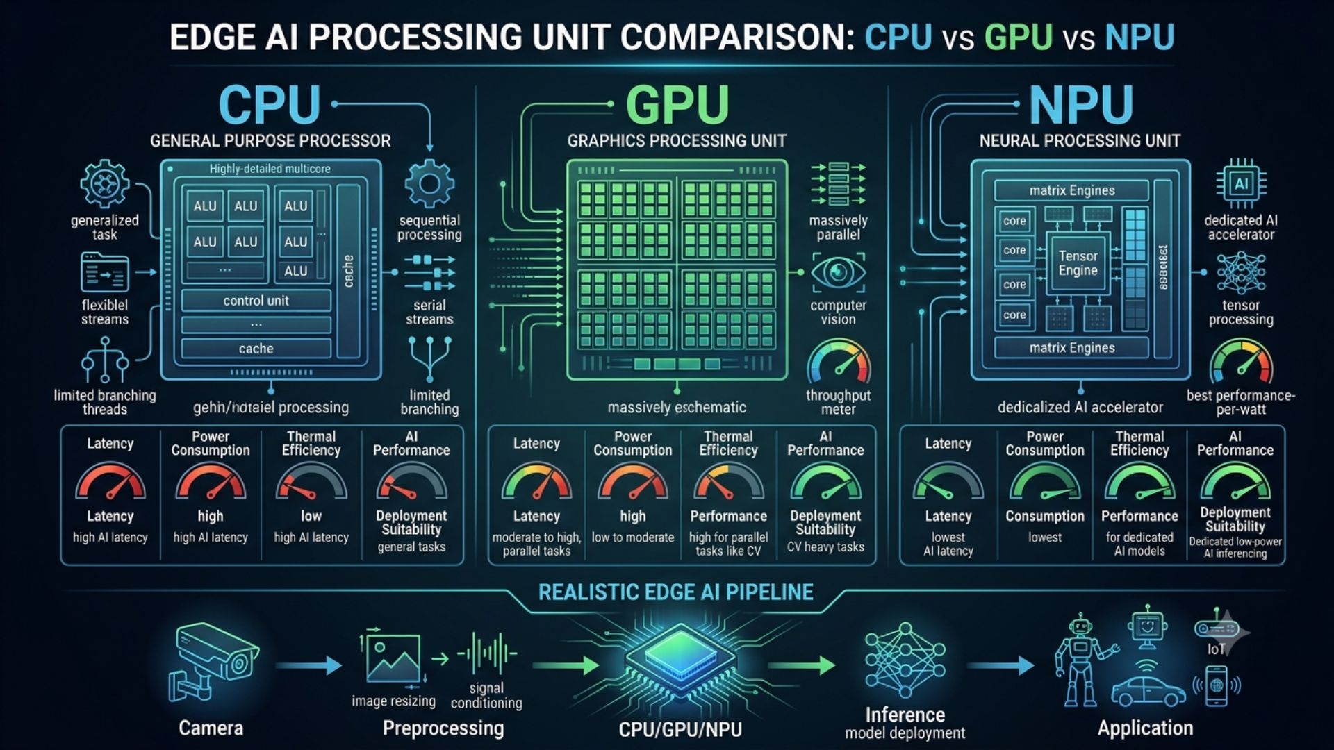
Dedicated Neural Processing Units have become an important part of this design strategy.
Unlike general-purpose CPUs, which are designed to handle a broad range of sequential and control-heavy workloads, NPUs are optimized for common operations found in neural networks. Depending on the architecture, those operations can include matrix multiplication, tensor processing, convolution, vector operations, and other stages of inference.
The hardware philosophy differs depending on where the accelerator will be used.
Mobile NPUs are usually integrated into larger System-on-Chip designs alongside CPUs, GPUs, memory controllers, image processors, and other specialized blocks.
That integration gives them access to a shared pool of power and thermal capacity.
A smartphone may use its NPU for many different jobs over the course of a day: computational photography, speech recognition, background noise processing, translation, augmented-reality features, or on-device generative AI. The hardware therefore needs a reasonable degree of programmability rather than being optimized for only one neural-network architecture.
Support for different numerical formats can also matter. Depending on the chip and software stack, an NPU may support formats such as INT8, INT16, FP16, or other precision modes.
Because the CPU, GPU, and NPU share the same package and thermal envelope, system software has to coordinate their workloads. Dynamic Voltage and Frequency Scaling (DVFS) is one of the tools used to adjust operating points according to workload demand and available thermal headroom.
The result is a system that may deliver very high AI performance for short periods while changing frequency and power levels as temperature and workload conditions evolve.
The other end of the spectrum consists of highly specialized inference accelerators and ASICs.
These chips are designed around particular workload characteristics rather than the broad application mix of a smartphone. They may devote a large portion of their silicon to matrix engines, systolic arrays, local memory, and other structures optimized for neural-network inference.
Quantized workloads are especially attractive because lower-precision arithmetic can reduce both computation cost and memory traffic when the hardware supports it efficiently.
The advantage is efficiency. A specialized accelerator can avoid some of the general-purpose control logic required by a CPU or programmable processor and devote more of its resources to the operations that matter for its target workload.
The trade-off is flexibility.
If a future model relies heavily on operators or numerical formats that the accelerator does not handle efficiently, software may have to fall back to another processor or accept lower performance. Edge ASIC design therefore involves a difficult prediction: which model operations will remain important over the useful life of the chip?

One of the easiest mistakes in edge AI design is to focus entirely on arithmetic throughput.
A neural network may perform millions or billions of mathematical operations during inference, but those operations are only part of the energy budget. Data has to reach the compute units first.
Model weights, activations, intermediate feature maps, and other tensors may move between different levels of the memory hierarchy. Accessing on-chip memory is generally much cheaper and faster than repeatedly transferring data to and from external DRAM, although the exact energy cost depends on the implementation.
This makes data movement a major efficiency constraint for many edge workloads.
One common strategy is to provide substantial on-chip SRAM.
Frequently accessed weights and intermediate data can remain close to the accelerator rather than being fetched repeatedly from external memory.
The amount of SRAM available is limited by silicon area and power considerations, so hardware designers have to decide which data should remain on-chip and which data can be streamed from lower levels of the memory hierarchy.
That decision can have a surprisingly large effect on real-world performance.
Quantization can reduce both model size and memory traffic.
For example, converting a model from higher-precision representations to INT8 or, where supported, lower-precision formats can reduce the number of bits required to store and move each parameter.
The benefit is not automatic. Accuracy can change, and the hardware and inference software must support the chosen format efficiently. But when those pieces line up, quantization can substantially improve the amount of useful inference that can be performed within a fixed power budget.
The strongest results often come from designing the model and hardware with each other in mind.
A neural network that looks efficient from a purely algorithmic perspective may perform poorly on a particular accelerator if its tensor shapes create inefficient memory access patterns or exceed the available local buffers.
Conversely, a model designed around the hardware's strengths can make much better use of the available compute and memory bandwidth.
This is why edge AI increasingly depends on co-design rather than treating software and silicon as completely separate layers.
Short inference bursts are relatively easy to accommodate because the device has time to return toward a lower temperature between workloads.
Continuous workloads are harder.
Consider a camera performing local computer vision throughout the day or an industrial controller processing a steady stream of sensor data in a warm environment. The device cannot simply run at its maximum clock speed indefinitely if the cooling system cannot remove the resulting heat.
As temperature increases, hardware may reduce voltage or frequency, migrate workloads, disable selected processing resources, or enter lower-power operating states.
Thermal management therefore involves more than a temperature sensor and a shutdown threshold.
Duty cycling can reduce average power by alternating periods of active computation with lower-power states when the workload permits.
This is particularly useful for sensors and devices that do not need continuous full-rate inference. Instead of keeping the accelerator active at a high frequency, the system can process data in bursts and spend the remaining time at much lower power.
The technique works best when the application can tolerate those timing patterns. A real-time workload with strict latency requirements has less freedom than a sensor that only needs to analyze an event every few seconds.
System software can also distribute work across different processing blocks.
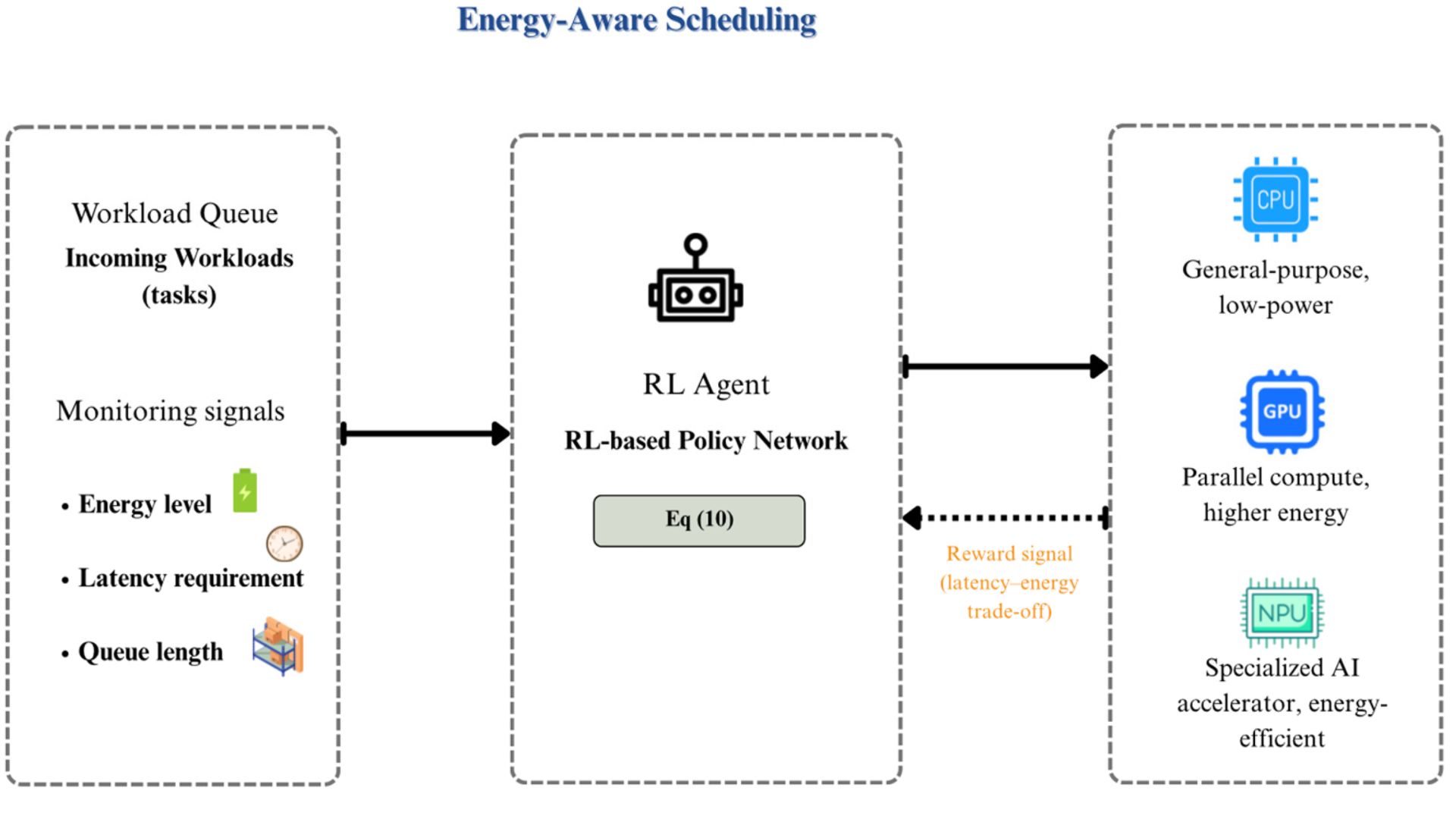
A heterogeneous SoC may have a CPU, GPU, NPU, image processor, and other accelerators. Not every task has to run on the same unit, and moving selected workloads between blocks can help balance performance, power, and temperature.
This becomes especially useful when the device has accumulated thermal load and no longer has the same headroom it had at the start of a workload.
Performance-per-watt is one of the most important metrics in edge AI, particularly when the device operates from a battery or within a tightly constrained thermal envelope.
But it is not the only one.
Engineers also have to consider inference latency, throughput, model compatibility, memory capacity, software support, accuracy, physical size, manufacturing cost, and long-term reliability.
A chip that delivers excellent TOPS-per-watt but cannot efficiently run the target model may be less useful than a slightly slower accelerator with better software support.
Similarly, a processor with excellent peak efficiency may be a poor choice if its sustained performance falls sharply once the device reaches its thermal limit.
For that reason, realistic evaluation should include sustained workloads rather than relying solely on short peak-performance tests.
Edge AI hardware works best when compute, memory, power, and thermal design are treated as one system.
A larger NPU may provide more theoretical throughput, but it can also increase silicon area and power consumption. More on-chip memory can reduce external memory traffic, but it consumes additional die area. Lower-precision arithmetic can improve efficiency, but it may require model changes and careful validation.
Every improvement has a cost somewhere else.
The same applies at the device level. A larger heat spreader may improve sustained performance but increase size and weight. More battery capacity can extend operating time but makes the product heavier. A more aggressive cooling solution can provide additional thermal headroom but may increase cost or complicate mechanical design.
The best edge AI designs are therefore not necessarily the ones with the highest specification on any single datasheet line.
They are the ones that keep the entire system within its practical limits.
Edge AI hardware faces a very different set of constraints from large cloud accelerators.
The processor has to deliver useful inference performance while sharing a limited power and thermal budget with the rest of the device. That makes sustained performance, memory efficiency, and power management just as important as peak compute throughput.
Mobile NPUs offer flexibility for workloads that change throughout the day, while specialized edge accelerators can achieve high efficiency when the target workload is well understood. On both platforms, minimizing unnecessary data movement can have a major impact on energy consumption, while quantization and on-chip memory can help reduce the pressure on external memory.
Thermal management completes the picture. A chip that performs well for a few seconds is not necessarily a well-designed edge processor if it cannot maintain that performance under the workload the device was built to handle.
As more AI inference moves from centralized servers into phones, cameras, vehicles, industrial equipment, and other connected devices, the most useful measure of hardware progress will not be raw compute alone. The real challenge is delivering enough intelligence, for long enough, within the power, temperature, memory, and physical limits of the device.