
Decoding the technologies of tomorrow, today.
Exploring the breakthrough innovations shaping our world. From AI infrastructure and robotics to biotech, quantum computing, and spatial tech.
Exploring the breakthrough innovations shaping our world. From AI infrastructure and robotics to biotech, quantum computing, and spatial tech.
For more than a decade, FinFET technology has been one of the foundations of advanced semiconductor manufacturing. Its three-dimensional fin structure gave the gate much better control of the transistor channel than earlier planar designs, helping chipmakers continue increasing transistor density while improving performance and energy efficiency. FinFET remains important today, but continued scaling has become harder. As advanced logic processes move toward smaller geometries, controlling leakage, power, interconnects, and manufacturing complexity requires more than simply shrinking the transistor.
That is why the industry's next steps involve several changes at once. At the transistor level, leading-edge processes are moving toward Gate-All-Around (GAA) architectures, often based on nanosheets. At the chip level, designers are increasingly using chiplets instead of putting every function onto one large monolithic die. Advanced 2.5D and 3D packaging then provides the high-density connections needed to bring those pieces together. Backside power delivery adds another layer of optimization by separating power distribution from much of the front-side signal routing.
These technologies address different problems, but they are increasingly being designed as parts of the same system.
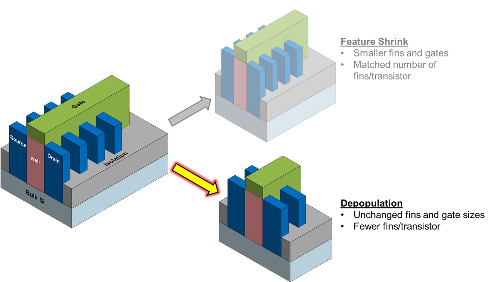
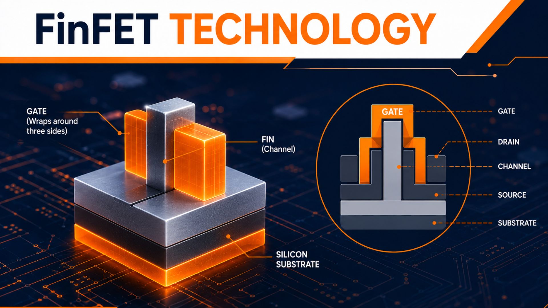
A FinFET surrounds the transistor channel on three sides with the gate. That geometry was a major improvement over traditional planar transistors because it gave the gate stronger control over the channel and helped reduce unwanted leakage as dimensions became smaller.
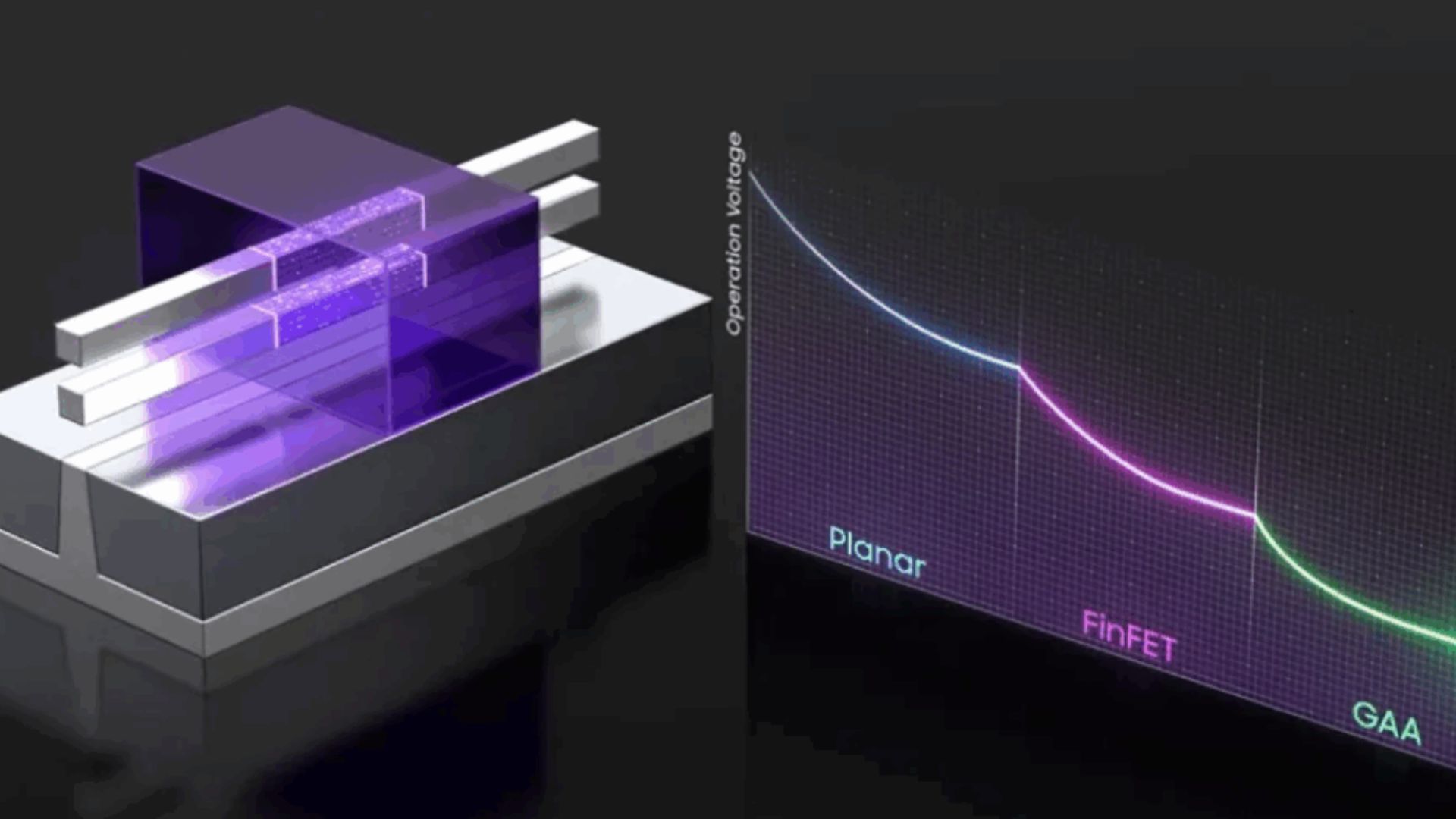
The challenge is that continued scaling makes electrostatic control increasingly difficult. Short-channel effects, leakage, power density, and the physical limitations of the fin geometry all become more important as designers push toward advanced process nodes. The transition to GAA is therefore less about a single "3-nanometer limit" and more about finding a transistor architecture that provides stronger control as scaling continues.
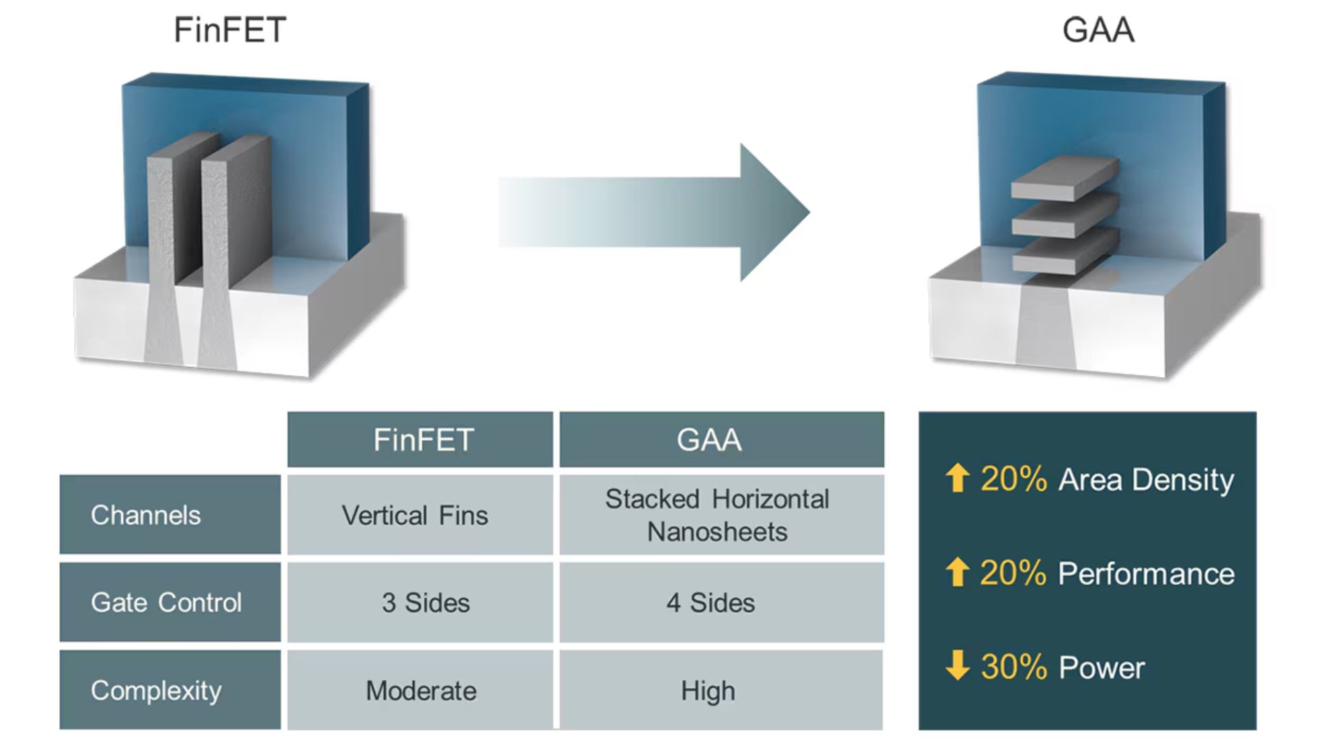
In a GAA design, the gate surrounds the channel on all sides. One widely used implementation employs stacked horizontal nanosheets, creating a structure in which the gate has much greater control over the current flowing through each channel. TSMC's N2 process, for example, uses its first generation of nanosheet transistor technology, while its N3 family continues to use FinFETs. This illustrates why transistor architecture should not be tied too rigidly to a particular node number.
GAA provides several important design advantages.
Stronger electrostatic control: Because the gate surrounds the channel, it can exercise tighter control over the transistor's on and off states. Better control can help reduce leakage and support continued scaling.
More flexible drive-current design: Nanosheet architectures give designers additional freedom to adjust channel dimensions. Wider sheets can provide greater drive current, while narrower structures can be used where power efficiency and area are more important.
A path for continued scaling: GAA does not eliminate the difficulties of advanced semiconductor manufacturing, but it gives process engineers another transistor architecture with which to balance performance, power, and density.
Intel's RibbonFET is one commercial example of a GAA implementation. Intel describes RibbonFET as providing improved electrostatic control, performance per watt, and scaling characteristics compared with traditional FinFET designs.
Better transistors help, but AI processors are running into another limitation: a single chip cannot simply grow indefinitely.
Large monolithic dies face reticle-field constraints in advanced lithography, along with rising manufacturing cost and defect sensitivity. A larger die contains more area that can potentially be affected by manufacturing defects, which makes yield increasingly important. The economics can become difficult long before a design reaches a theoretical physical boundary.
AI processors make the problem particularly visible because they may need enormous numbers of transistors, large memory interfaces, high-speed interconnects, cache, I/O circuitry, and specialized compute resources. Putting all of those functions onto one monolithic die can be attractive from an interconnect perspective, but the manufacturing and design trade-offs become increasingly difficult as the die grows.
That is where chiplets enter the picture.
A chiplet-based processor divides a large design into multiple dies, with each die handling a particular function. Compute chiplets, I/O dies, cache dies, memory interfaces, and other components can be manufactured and optimized separately before being combined into one package.
The approach offers an important economic advantage. Not every function needs the most advanced and expensive process technology. High-performance compute logic may benefit from a leading-edge node, while I/O or other supporting circuits may be perfectly suited to a more mature process. Chiplets allow those functions to be designed and manufactured more independently.
AMD has used chiplet architectures extensively in its processor families, and its current CDNA architecture for AI and HPC continues to combine chiplets with HBM and high-bandwidth on-package interconnects. AMD describes its newer AI architecture as partitioning compute, memory, cache, and I/O functions across specialized dies.
The trade-off is complexity. Once a processor is split across several dies, the package itself becomes part of the system architecture. Communication between chiplets has to be fast, power-efficient, reliable, and dense enough to avoid creating a new bottleneck.
One common approach is 2.5D integration. Instead of stacking every die vertically, several dies are placed side by side on an advanced package substrate, silicon interposer, or bridge structure. Dense wiring within the package provides connections between compute dies, memory, and other components.
This architecture is particularly valuable for AI processors because memory bandwidth has become as important as raw compute capacity. High Bandwidth Memory, or HBM, can sit close to the compute logic and communicate through very dense package-level connections.
The result is a different way of thinking about processor design. The package is no longer simply a container for the chip. It becomes part of the interconnect fabric that determines how quickly compute units can exchange data with memory and with one another.
AMD's current CDNA materials provide a good example of this approach. The company's AI architecture combines multiple compute chiplets, HBM, I/O dies, and advanced packaging to provide the bandwidth required by large AI workloads.
2.5D packaging keeps most dies on roughly the same horizontal plane. 3D integration takes another approach by stacking dies vertically.
The attraction is straightforward: vertical integration can place related functions much closer together while dramatically increasing interconnect density. Instead of consuming additional board or package area to add another component, designers can place one die above another.
The technology can take several forms. Through-Silicon Vias (TSVs) provide vertical electrical connections through silicon, while newer approaches such as hybrid bonding can create extremely dense die-to-die connections without relying solely on conventional micro-bump structures.
AMD's 3D V-Cache technology, for example, uses TSVs and direct copper-to-copper bonding for silicon-to-silicon communication.
The benefits come with trade-offs. Heat becomes harder to remove when active silicon is stacked vertically, manufacturing and bonding become more complicated, and yield must be considered across multiple dies and assembly steps. Power delivery also becomes more demanding. Three-dimensional integration therefore improves density and connectivity, but it does not remove the underlying engineering constraints.
As transistor density rises, power delivery itself can become a limiting factor.
Traditional designs route both power and signals through the front side of the die. Those networks compete for valuable wiring resources, creating congestion and adding resistance. Under heavy workloads, the voltage delivered to parts of the chip can also fall below the ideal level, a phenomenon commonly referred to as IR drop or voltage droop.
Backside power delivery changes the arrangement. Instead of forcing power and signal networks to share the same routing environment, the power network is moved toward the back of the wafer or die. This leaves more front-side wiring resources available for signals while providing a more direct path for power delivery.
Intel's PowerVia technology is one example. Intel says its backside power architecture reduces interconnect congestion and IR drop while improving power delivery for advanced designs.
TSMC is pursuing a related direction as well. Its A16 technology combines nanosheet transistors with a backside power rail solution, illustrating how transistor architecture and power delivery are increasingly being developed together.
The significance for AI processors is straightforward: increasingly dense compute hardware needs increasingly sophisticated power infrastructure. Better transistor performance alone is not enough if the surrounding power network cannot deliver current efficiently during demanding workloads.
It is easy to describe GAA, chiplets, 2.5D packaging, 3D integration, and backside power delivery as separate semiconductor trends. In practice, they address different layers of the same scaling problem.
GAA transistors address transistor-level scaling. They improve electrostatic control and provide another path for improving performance, power, and density as conventional FinFET scaling becomes more difficult.
Chiplets address die-level scaling. Instead of making one enormous monolithic processor, designers can divide the system into smaller functional dies.
Advanced packaging addresses communication. Interposers, bridges, hybrid bonding, and other technologies allow those dies to exchange data at much higher bandwidth than conventional board-level connections.
Backside power delivery addresses power distribution. Moving power routing away from much of the front-side signal network can reduce congestion and improve the delivery of current to dense logic.
The important point is that none of these technologies works in isolation. A leading-edge AI processor may combine an advanced transistor architecture with chiplets, HBM, sophisticated package-level interconnects, and a new power-delivery structure.
The semiconductor industry's transition beyond FinFET is not a single architectural switch. It is a broader shift in how engineers think about scaling.
At the transistor level, GAA provides better control over increasingly small channels. At the die level, chiplets provide a practical way to build larger and more specialized processors without relying entirely on enormous monolithic dies. At the package level, 2.5D and 3D technologies provide the bandwidth needed to connect those pieces. And at the power-delivery level, backside architectures create additional room for the electrical infrastructure required by dense computing.
AI is pushing all of these constraints at once. More compute creates demand for more transistors, more memory bandwidth, more interconnect capacity, and more power. The response is therefore not simply a smaller transistor. It is a layered approach in which process technology, chip architecture, packaging, memory, and power delivery are optimized together.
That is the real story beyond FinFET: semiconductor scaling is increasingly becoming a system-level engineering problem, not just a transistor-sizing exercise.